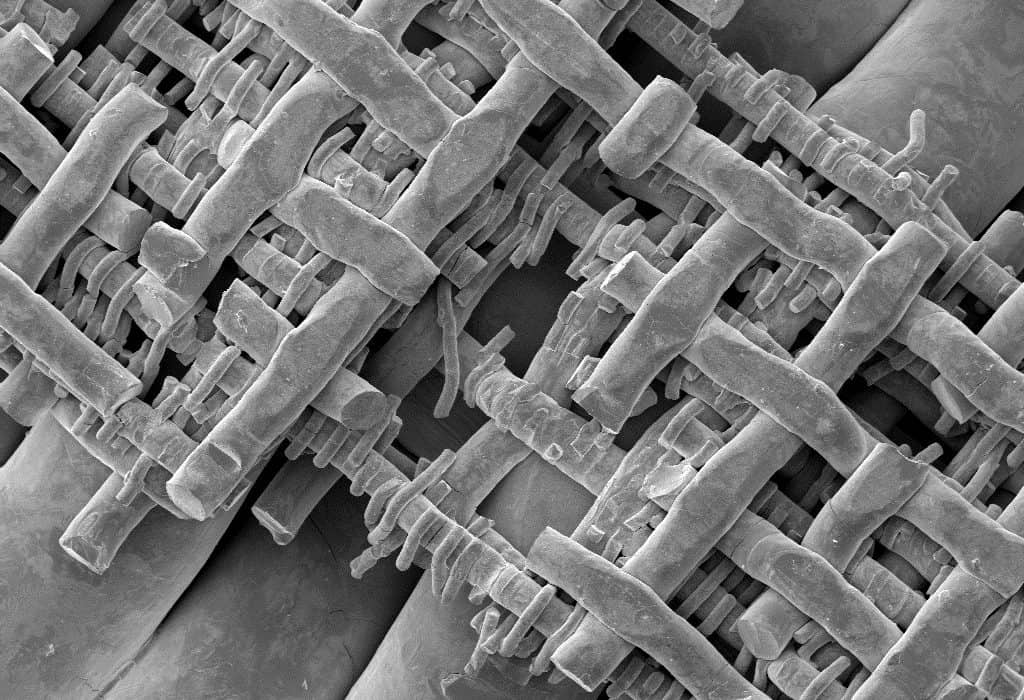
Scanning electron microscopy (SEM)
The scanning electron microscope (SEM) is a general-purpose tool for research, development, quality assurance and damage analysis. Components, assemblies and fracture surfaces can be examined for material composition and surface structure.
High resolution and analysis
In scanning electron microscopy, a finely focused electron beam is guided in a line over the surface of the object under investigation. The electron stream backscattered by the sample is recorded and displayed on the screen. The main advantage of scanning electron microscopy is its high resolution combined with great depth of field. Magnifications of up to approx. 50,000 times can be achieved. In addition to the exact representation of the surface topography, local differences in the sample composition can also be made visible. Elements from atomic number 6 (incl. O, C and N) can be detected qualitatively to semi-quantitatively.
Application examples:
- Characterization of materials and surfaces
- Investigation of fracture surfaces from damage events
- Quality control of components and parts
- Determination of the chemical composition of very small samples
In addition to the exact representation of the surface topography, differences in the material composition of the sample can also be made visible. By means of energy dispersive X-ray analysis (EDX), elements with an atomic mass of 6 and higher (i.e. including O, C and N) can be analyzed qualitatively and semi-quantitatively. In the large sample chamber, samples and components up to 200 mm in diameter and 50 mm in height can be analyzed. The SEM is equipped with one of the most advanced EDX spectrometers.

